WHAT IS CC1125 ?
The CC1125 device is a fully integrated single-chip radio transceiver designed for high performance at very low-power and low-voltage operation in cost-effective wireless systems. All filters are integrated, thus removing the need for costly external SAW and IF filters. The device is mainly intended for the ISM (Industrial, Scientific and Medical) and SRD (Short Range Device) frequency bands at 164–192 MHz, 274–320 MHz, 410–480 MHz, and 820–960 MHz.
The CC1125 device provides extensive hardware support for packet handling, data buffering, burst transmissions, clear channel assessment, link quality indication, and Wake-On-Radio. The main operating parameters of the CC1125 device can be controlled through an SPI interface. In a typical system, the CC1125 device will be used with a microcontroller and only a few external passive components.
SCHEMATIC AND BOARD DESIGN
The task was to design a 4-layer RF PCB for the peripheral circuit of CC1125 for 435 MHz band. All layers are grounded except the third layer which is defined as VCC layer. On the first and fourth layer, signal traces were placed.
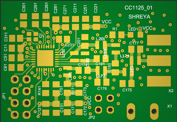
Following is a schematic diagram made in EAGLE.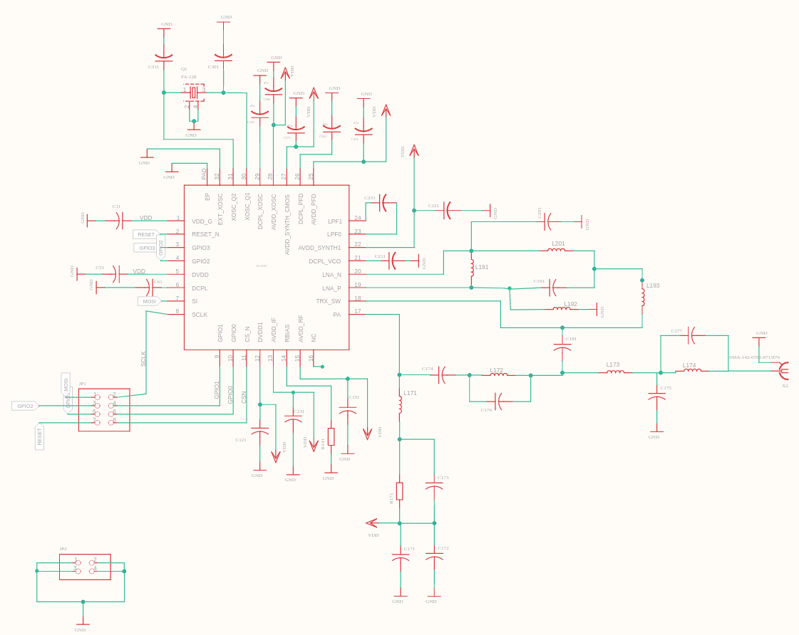 The board design and printed PCB are shown as follows. The red traces are on the first layer whereas the blue traces are on the fourth layer.
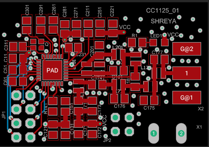
The soldering and testing of PCB will be done after the lockdown is over.
Shown below is a CC1125 BoostXl development board available in the market. Although it comes with an inbuilt microcontroller, one can connect an external microcontroller as well.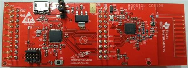
RF PCB GUIDELINES
Certain guidelines were kept in mind while designing the 4-layer RF PCB as follows:
- All layers are defined as GND except the third layer which is the VCC.
- There are three signals on the PCB - digital, RF (which actually carries our signal) and power signal (connected to VCC). Traces of RF and VCC signals are made thicker.
- According to the DRC layer specifications, by using Saturn PCB toolkit, the thickness of the RF traces is determined (keeping impedance as 50 ohms). The trace width is calculated by considering board as microstrip passive circuit or coplanar passive circuit.
- The digital traces thickness is kept equal to the pad width of the IC.
- For RF signals, the width of the trace is changed only after the first element from the pad or clearance issues will come.
- While routing, the RF traces are made straight and small in most of the cases. Vias are put in the empty spaces around the RF traces and are grounded by changing the name.
- The decoupling capacitors are placed close to each other and the IC. The oscillator is also placed near the IC.
- RF routing is preferred to be done in one layer.
- The traces that are VCC signals are made to be the thickest one. It is decided according to the amount of current circuit draws.
- The drill size of the vias is equal to the trace size in the corresponding traces.
- The middle pad of the IC is grounded using a lot of grounded vias.
- A few vias are needed to check the voltage at certain points. The stop property is applied to prevent soldermask to cover the via, and thus voltage can be checked using a multimeter.